October 11, 2026
Low-Power AI Accelerators and FPGAs: Inside Apex Compute's Unified Engine
edge-ai · fpga · ai-accelerator · low-power · benchmarks
Every edge AI vendor ships a TOPS number. Almost none ship a joules-per-token number. That is a problem, because when a drone, a robot arm or an on-premises box actually runs a transformer, the two numbers that decide whether the system works are energy per token and latency — not the marketing peak on the datasheet.
This is the lens I use to look at Apex Compute, a Los Altos company (founded 2024) building a transformer-focused AI accelerator they call the Unified Engine. It runs on off-the-shelf FPGAs today, with a 12nm ASIC tape-out in progress. Their claims are unusually specific — and reproducible on GitHub. So let’s measure the claims.
Why FPGAs still matter at the edge
The edge accelerator market is crowded: fixed-function ASICs (Hailo, Axelera, SiMa.ai), NPUs inside application processors, tiny neuromorphic chips, and FPGAs. FPGAs occupy a specific niche:
- Reconfigurability. The datapath can be reprogrammed after manufacturing. When a model family shifts — as it did from CNNs to transformers, and again toward VLA (vision-language-action) architectures — an FPGA can be re-optimized instead of replaced.
- Pre-silicon validation. For a startup taping out custom silicon, running the real RTL on FPGA fabric is how you find bugs before spending millions on masks.
- Deterministic latency. No scheduler surprises, no shared caches with a GPU driver stack. For control loops in robotics and vehicles, bounded latency is a feature.
The classic objection — FPGAs are slow and power-hungry compared to ASICs — is real. Which is exactly why a claim like “one FPGA engine at 333 MHz competes with shipping 8nm ASICs” deserves a careful look.
Inside the Unified Engine
Apex’s design thesis is simple: transformers are not general matrix machines. They are a narrow set of operators — matmul, softmax, element-wise ops, quantized attention — repeated thousands of times. So the Unified Engine is a single compute engine combining matrix and vector paths, with those operators implemented close to peak efficiency instead of squeezed through a general-purpose pipeline.
The published FPGA prototype on a Xilinx Kintex UltraScale+ (KU5P) reports:
| Metric | Prototype figure |
|---|---|
| Logic footprint | 78,348 CLB LUTs, 50,045 registers |
| DSP slices | 197 |
| On-chip memory | 1.05 MB SRAM (30 URAM / 16 BRAM tiles) |
| Timing closure | 366 MHz on 16nm fabric |
| Peak compute | 47 GFLOPS BF16 |
| Matrix utilisation | up to 95.6% of peak |
| Precision formats | BF16, FP8, INT8, INT4, FP4, block-quantized TQ4 |
Two details stand out. First, utilisation: 95% of theoretical peak on M=K=N=1024 matmul (40.17 of 42 GFLOPS) is excellent; most FPGA accelerators live in the 30–60% range because the datapath stalls on memory. Second, fused kernels: the attention kernel runs Q·Kᵀ, scaling, bias, softmax and the value matmul in a single pass — 36.87 GFLOPS peak at sequence length 3072, 87.8% of theoretical. Every kernel you fuse is a round-trip to DRAM you don’t pay for, and at the edge that is where the watts go.

Benchmarks: Gemma 3 1B, head to head
The headline comparison is against NVIDIA’s Jetson Orin Nano 8GB — the default reference board for edge AI. Apex ran Gemma 3 1B decode through llama.cpp (CUDA, one CPU thread on the Jetson):
| Apex · Kintex KU5P | Jetson Orin Nano | |
|---|---|---|
| Process | 16nm FPGA fabric | 8nm ASIC |
| Memory | 32-bit DDR4 @ 1333 MHz | 128-bit LPDDR5 @ 2133 MHz |
| Power | 4.5 W total | 7 W compute module |
| Decode speed | 15.63 tokens/s | 7.59 tokens/s |
| Energy per token | 0.287 J | 0.922 J |
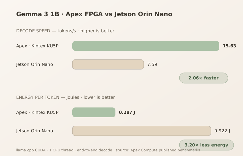
That is 2.06× faster decoding and 3.20× better energy per token — from a device with a third of the memory bandwidth, on an older process node. The per-operator breakdown explains where the win comes from: RMSNorm 27×, RoPE 6.75×, attention internals up to 20×, large matrix-vector products 3.12× versus CUDA. Softmax, element-wise ops and normalisations are exactly the operations GPUs handle worst per watt, and exactly what transformer decode is made of.
For calibration: the same model on PyTorch CUDA on the Jetson hits 2.9 tokens/s — the Apex engine is 5.2× faster than that. The comparison is fair in one direction (both run end-to-end, llama.cpp is the best practical CUDA stack) and rough in another (a 16nm FPGA beating an 8nm ASIC on energy is an architecture win, not a process win).
Against shipping edge ASICs
The more interesting frame is normalised throughput versus accelerator modules you can buy today, on Llama 3.2 1B / Gemma 3 1B / Gemma 4 E2B:
| Platform | Type | Normalised throughput |
|---|---|---|
| NVIDIA Jetson Orin Nano | 8nm ASIC, shipping | 1× |
| Axelera Metis AIPU | 4 cores @ 800 MHz, shipping | 2.2× |
| SiMa.ai Modalix | MLSoC, shipping | 2.4× |
| Apex Unified Engine | 1 engine @ 333 MHz, FPGA | 2× |
| Apex 12nm ASIC (projected) | 32 engines @ 1.6 GHz | 20× |
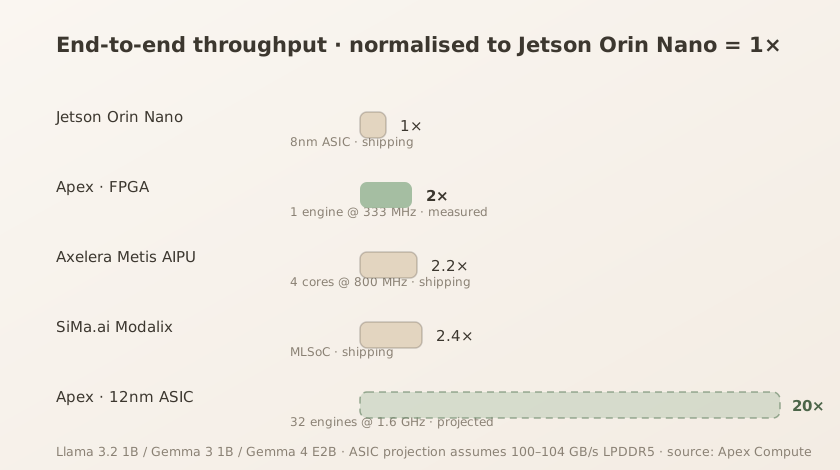
One Apex engine at a third of the clock of these shipping parts reaches ~90% of Axelera’s and ~82% of SiMa.ai’s end-to-end throughput. Read that carefully: it says the architecture’s efficiency per clock is high, and it also says the FPGA prototype is not yet beating shipping silicon outright. The 20× claim lives in the ASIC projection — and projections are where honest engineering needs a footnote.
The 12nm roadmap — and how to read it
Apex’s stage two is a GlobalFoundries 12nm edge-AI SoC, with MIPS as the system-architecture partner: 32 engines at 1.6 GHz, LPDDR5 at ~104 GB/s, target under 10 W. The projected system speedup is ≥20× over Jetson.
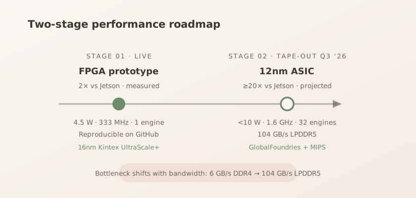
How should you read a projected number? Check the constraints they state. Apex is explicit: the design is memory-bandwidth-bound on weight matmul and compute-bound on SRAM-resident operations, with no structural bottleneck between. That is the right way to publish a simulation — name the bottleneck. The 12nm engine assumes 10× the bandwidth of the current DDR4 setup; if LPDDR5 delivery falls short, the projection falls with it. The two-engine, 6 GB/s DDR scenario behind the FPGA numbers is reproducible from their public repository, which is more transparency than most vendors offer.
Software is half the hardware
Edge accelerators die of software more often than of silicon. Apex’s stack has three pragmatic choices worth noting:
- One compiled prefill program handles any prompt up to 192 tokens, cutting the instruction binary ~10×. Fewer binaries to ship, fewer to validate.
- Per-block quantization: INT4 or NVFP4 is chosen per 64-element K-block by minimising MSE, while norms and embeddings stay in BF16. This is the trick that makes 4-bit inference look like 8-bit accuracy — quantize where the tolerance is, not uniformly.
- Field updates without a reboot: one command reflashes the fabric, warm-boots and re-scans PCIe. In production fleets, “no power cycle” is an underrated feature.
Text, vision, speech and localization models (Qwen, Llama, Gemma, VLA workloads) reportedly run on the prototype under an automated test suite.
Where this matters
The stated targets — drones, autonomous vehicles, robotics, off-cloud installations — are the places where a joule saved is flight time or battery life, and where data cannot leave the building. For onboard spacecraft-adjacent and remote compute, the same equation applies at a harsher constant: every watt is thermal budget you must reject somewhere.
A checklist for evaluating any low-power accelerator
If you are comparing edge inference hardware — Apex or anyone — measure these, in this order:
- Joules per token (or per frame) on your model, end to end — not kernel peaks.
- Utilisation percentage on your operator mix. Under 60% on matmul means the datapath is stalling.
- What the numbers assume — memory bandwidth, batch size, precision, quantization scheme.
- Reproducibility — is there a repo? Can you re-run it?
- Update path — how do a thousand deployed devices get a new model? The same habit decides whether a home server stays safe over time. I measured what six months of missed updates costs in Built and Abandoned Systems.
FAQ
Is an FPGA really more efficient than a GPU for LLM inference? For transformer decode at batch size 1 on the edge — where operators like softmax, RMSNorm and small matvecs dominate — a specialised datapath can beat a general GPU per watt, as Apex’s 3.2× energy advantage over Jetson Orin Nano illustrates. For large-batch training, GPUs remain unmatched.
What is block-quantized TQ4/INT4? Instead of quantizing a whole tensor with one scale, the hardware picks precision per block (Apex: per 64-element K-block) by minimising reconstruction error. Accuracy holds up while memory traffic drops.
Does the 20× ASIC projection prove anything? It proves the architecture scales when bandwidth scales. The honest signal is the FPGA prototype’s measured 2× at 333 MHz plus named bottlenecks. Treat the 20× as a hypothesis with a tape-out date (Q3 2026), not a result.
Can I verify the benchmarks myself? Yes — the RTL, runtime and Gemma 3 1B example are public on GitHub (apex-compute/unified-engine), and the FPGA prototype card is available for licensing. Reproducibility is the single best credibility signal in this market.
FPGA or ASIC for my edge product? If your model mix will change in 18 months — likely, given VLA and multimodal momentum — FPGA or reconfigurable IP buys insurance. If the workload is frozen and volume is high, ASIC wins on cost and power.
Performance figures in this post are Apex Compute’s published numbers (apexcompute.com), measured end-to-end unless noted; projections are clearly marked. Always re-measure on your own model and power envelope before committing a design.